With the increase in power density brought by the development of semiconductor devices toward miniaturization and high integration, the heat generated by electronic equipment is getting larger and larger, and thermal failure has become the primary problem that hinders the performance and life of electronic equipment. According to statistics, every time the temperature of an electronic device increases by 10 ° C-15 ° C, its corresponding service life will be reduced by 50%. Efficient thermal management technology is the key to solving this problem. One of the effective methods is to fill a layer of thermal interface material between the heat source and the heat sink. Thermal interface materials with excellent performance need to have both high thermal conductivity and good compressibility, but these two characteristics are difficult to meet at the same time. For example, most metals have a high thermal conductivity (70Wm-1K-1–400m-1K-1), but their compression modulus is also very high (70GPa–120GPa), making it difficult to fill the gap between the heating chip and the heat sink; and Although silica gel has a very low compressive modulus (0.3MPa–2MPa), its thermal conductivity is only 0.1m-1K-1–0.3m-1K-1, which makes it difficult to meet the requirements of thermal interface materials for longitudinal heat conduction. Although the addition of highly thermally conductive fillers to silica gel can increase the thermal conductivity, it also increases the compression modulus. According to relevant literature reports, after adding vertically aligned carbon nanotube arrays to PDMS, the out-of-plane thermal conductivity increased to 25m-1K-1, but the compression modulus also increased to 10MPa. Therefore, it is particularly important to develop thermal interface materials with both high thermal conductivity and low compressive modulus.
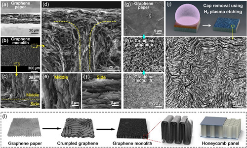
Recently, the functional carbon material team of the Surface Division of the Ningbo Institute of Materials Technology and Engineering, the Chinese Academy of Sciences has prepared a thermal interface material with high thermal conductivity and low compressive modulus based on a vertically arranged graphene structure. The preparation process of the material is shown in Fig. 1: applying transverse mechanical force to the graphene paper drawn by suction to make the graphene have a pleated structure, and then applying pressure to obtain a dense graphene thermal pad. This method changes the orientation of graphene paper from horizontal to vertical, and realizes the transition from horizontal heat transfer to vertical heat transfer of graphene paper.
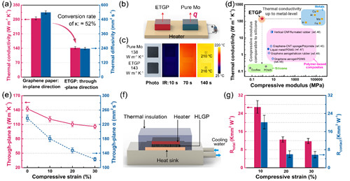
Figure 2 (a–k) shows the morphology of the graphene thermal pad at various stages during the preparation process. The final graphene thermal pad exhibits a multilayer structure on the microscopic level, with the vertical arrangement of graphene in the middle, top and bottom There is a thin layer of graphene arranged horizontally, and the overall structure is similar to a honeycomb plate (see Figure 2 (l)). The in-plane thermal conductivity of the graphene paper used as the raw material in the experiment is 273m-1K-1, and the longitudinal thermal conductivity of the graphene thermal pad obtained after structural conversion is 143m-1K-1 (conversion rate of 52%) , Has surpassed most metals (such as Mo, Zn, In, Ni, Fe, etc.), the corresponding results are shown in Figure 3 (a–d). In addition to having a high thermal conductivity, the graphene thermal pad also has a compression modulus equivalent to silica gel, which is only 0.87MPa, which is much lower than that of metal materials (Figure 3d), which is conducive to deformation during packaging and achieves lower contact Thermal resistance. At 30% compression rate, the out-of-plane thermal conductivity of the graphene thermal pad still exceeds 100m-1K-1, and the contact thermal resistance is as low as 5.8Kmm2 W-1, as shown in Figure 3 (e–g).
In the actual thermal interface performance evaluation experiment, the temperature drop of the system heat source with graphene thermal pad as the thermal interface material reached 65 ℃, much higher than the temperature drop (38 ℃) achieved by the application of commercial thermal interface materials. The experimental results are shown in the figure. 4 (a–c). Figure 4 (d–e) is the simulation of the heat dissipation process by the CFD simulation software. The results show that the contact thermal resistance of the graphene thermal pad is lower than that of mainstream commercial thermal pads. In Figure 4f, the graphene thermal pad exhibits good thermal cycling stability. After 2,500 thermal shock tests, the thermal performance fluctuation is less than 0.5%; in addition, the graphene thermal pad also has long-term stability Performance, working continuously at a power of 20Wcm-2 for 7 days, the difference between the heating plate and the ambient temperature did not change significantly (Figure 4g), showing good thermal shock stability and long-range stability. Related work has been published in ACS Nano (2019, DOI: 10.1021 / acsnano.9b05163). The research work was supported by the National Key Research and Development Program (2017YFB0406000), the Chinese Academy of Sciences Strategic Priority Research Program (XDA22000000), the Chinese Academy of Sciences Equipment (YZ201640), Ningbo City Special Projects (2016S1002 and 2016B10038), and Ningbo International Cooperation (2017D10016).

Figure 1 Preparation process of graphene thermal pad

Figure 2 Morphology of graphene thermal pad

Figure 3 Thermal conductivity and thermal resistance of graphene thermal pad

Figure 4 Thermal interface performance test and simulation of graphene thermal pad
Blue Tube Uv Light,Small Uv Light,Uv Flood Light,Single Ended Uv Lamp
Guangdong Kingrate Optoelectronic Technology Co., Ltd. , https://www.kingrateuv.com